- 您现在的位置:买卖IC网 > Sheet目录342 > MCBSTM32EXL (Keil)BOARD EVALUATION FOR STM32F103ZE
�� �
�
�Advanced-control� timers� (TIM1&TIM8)�
�RM0008�
�13.3.11�
�Complementary� outputs� and� dead-time� insertion�
�The� advanced-control� timers� (TIM1&TIM8)� can� output� two� complementary� signals� and�
�manage� the� switching-off� and� the� switching-on� instants� of� the� outputs.�
�This� time� is� generally� known� as� dead-time� and� you� have� to� adjust� it� depending� on� the�
�devices� you� have� connected� to� the� outputs� and� their� characteristics� (intrinsic� delays� of� level-�
�shifters,� delays� due� to� power� switches...)�
�You� can� select� the� polarity� of� the� outputs� (main� output� OCx� or� complementary� OCxN)�
�independently� for� each� output.� This� is� done� by� writing� to� the� CCxP� and� CCxNP� bits� in� the�
�TIMx_CCER� register.�
�The� complementary� signals� OCx� and� OCxN� are� activated� by� a� combination� of� several�
�control� bits:� the� CCxE� and� CCxNE� bits� in� the� TIMx_CCER� register� and� the� MOE,� OISx,�
�OISxN,� OSSI� and� OSSR� bits� in� the� TIMx_BDTR� and� TIMx_CR2� registers.� Refer� to� Table� 73:�
��page� 310� for� more� details.� In� particular,� the� dead-time� is� activated� when� switching� to� the�
�IDLE� state� (MOE� falling� down� to� 0).�
�Dead-time� insertion� is� enabled� by� setting� both� CCxE� and� CCxNE� bits,� and� the� MOE� bit� if� the�
�break� circuit� is� present.� There� is� one� 10-bit� dead-time� generator� for� each� channel.� From� a�
�reference� waveform� OCxREF,� it� generates� 2� outputs� OCx� and� OCxN.� If� OCx� and� OCxN� are�
�active� high:�
�●�
�●�
�The� OCx� output� signal� is� the� same� as� the� reference� signal� except� for� the� rising� edge,�
�which� is� delayed� relative� to� the� reference� rising� edge.�
�The� OCxN� output� signal� is� the� opposite� of� the� reference� signal� except� for� the� rising�
�edge,� which� is� delayed� relative� to� the� reference� falling� edge.�
�If� the� delay� is� greater� than� the� width� of� the� active� output� (OCx� or� OCxN)� then� the�
�corresponding� pulse� is� not� generated.�
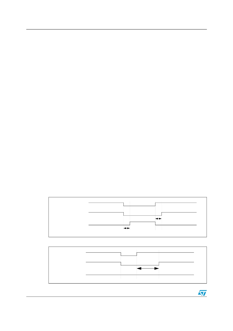
�The� following� figures� show� the� relationships� between� the� output� signals� of� the� dead-time�
�generator� and� the� reference� signal� OCxREF.� (we� suppose� CCxP=0,� CCxNP=0,� MOE=1,�
�CCxE=1� and� CCxNE=1� in� these� examples)�
�Figure� 85.� Complementary� output� with� dead-time� insertion.�
�OCxREF�
�OCx�
�delay�
�OCxN�
�delay�
�Figure� 86.� Dead-time� waveforms� with� delay� greater� than� the� negative� pulse.�
�OCxREF�
�OCx�
�delay�
�OCxN�
�278/995�
�Doc� ID� 13902� Rev� 9�
�发布紧急采购,3分钟左右您将得到回复。
相关PDF资料
MCBTMPM330
BOARD EVAL TOSHIBA TMPM330 SER
MCIMX25WPDKJ
KIT DEVELOPMENT WINCE IMX25
MCIMX53-START-R
KIT DEVELOPMENT I.MX53
MCM69C432TQ20
IC CAM 1MB 50MHZ 100LQFP
MCP1401T-E/OT
IC MOSFET DRVR INV 500MA SOT23-5
MCP1403T-E/MF
IC MOSFET DRIVER 4.5A DUAL 8DFN
MCP1406-E/SN
IC MOSFET DVR 6A 8SOIC
MCP14628T-E/MF
IC MOSFET DVR 2A SYNC BUCK 8-DFN
相关代理商/技术参数
MCBSTM32EXLU
功能描述:开发板和工具包 - ARM EVAL BOARD + ULINK2 FOR STM32F103ZG
RoHS:否 制造商:Arduino 产品:Development Boards 工具用于评估:ATSAM3X8EA-AU 核心:ARM Cortex M3 接口类型:DAC, ICSP, JTAG, UART, USB 工作电源电压:3.3 V
MCBSTM32EXLU-ED
制造商:ARM Ltd 功能描述:KEIL STM STM32EXL EVAL BOARD
MCBSTM32EXLUME
功能描述:开发板和工具包 - ARM EVAL BOARD + ULINKME FOR STM32F103ZG
RoHS:否 制造商:Arduino 产品:Development Boards 工具用于评估:ATSAM3X8EA-AU 核心:ARM Cortex M3 接口类型:DAC, ICSP, JTAG, UART, USB 工作电源电压:3.3 V
MCBSTM32F200
功能描述:开发板和工具包 - ARM EVAL BOARD FOR STM STM32F207IG
RoHS:否 制造商:Arduino 产品:Development Boards 工具用于评估:ATSAM3X8EA-AU 核心:ARM Cortex M3 接口类型:DAC, ICSP, JTAG, UART, USB 工作电源电压:3.3 V
MCBSTM32F200U
功能描述:开发板和工具包 - ARM EVAL BOARD FOR STM STM32F207IG + ULINK2
RoHS:否 制造商:Arduino 产品:Development Boards 工具用于评估:ATSAM3X8EA-AU 核心:ARM Cortex M3 接口类型:DAC, ICSP, JTAG, UART, USB 工作电源电压:3.3 V
MCBSTM32F200UME
功能描述:开发板和工具包 - ARM EVAL BOARD FOR STM STM32F207IG ULINK-ME
RoHS:否 制造商:Arduino 产品:Development Boards 工具用于评估:ATSAM3X8EA-AU 核心:ARM Cortex M3 接口类型:DAC, ICSP, JTAG, UART, USB 工作电源电压:3.3 V
MCBSTM32F200UME-ED
制造商:ARM Ltd 功能描述:KEIL STM32F207IG EVAL BOARD
MCBSTM32F400
功能描述:开发板和工具包 - ARM EVAL BOARD FOR STM STM32F407IG
RoHS:否 制造商:Arduino 产品:Development Boards 工具用于评估:ATSAM3X8EA-AU 核心:ARM Cortex M3 接口类型:DAC, ICSP, JTAG, UART, USB 工作电源电压:3.3 V